Magical Calibration
MAG*I*CAL traceable TEM calibration standard
Introduction
 |
|
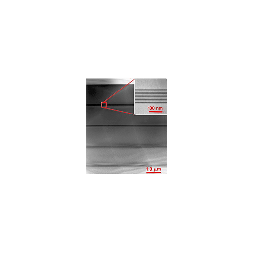
TEM image of four identical structures with alternating Si/SiGe lines. |
|
|
|
Diagram of the four regions of the calibration structures |
An accurately calibrated TEM is imperative for generating correct imaging data. With the traceable MAG*I*CAL calibration standard, the TEM can be accurately calibrated. The MAG*I*CAL traceable TEM calibration standard consists of 4 sets of 5 SiGe layers with a thickness of ~10nm, alternating with pure silicon layers with a thickness of ~13nm. The total thickness of the set of alternating layers is ~100nm. The distance between each set of 5 layers is ~1.2µm. The epitaxial layers are grown using an MBE (Molecular Beam Epitaxy) process on a single crystal silicon {001} substrate. The finished calibration standard is a cross-sectioned TEM calibration sample with four regions where the calibration lines can be imaged.
The unique MAG*I*CAL TEM magnification calibration standard can be used to calibrate:
- The TEM over the entire range from 1000x up to 1,000,000x magnification with the alternating lines
- Camera constant calibration using the Si single crystal
- Image / diffraction pattern rotation calibration using the Si single crystal area
The four sets of alternating layers of Si and SiGe provide light and dark lines with good contrast. These four sets of the alternating layers are calibrated using a high resolution transmission electron microscope (HR-TEM) with reference to the {111} lattice space of silicon (0.3135428nm) measured on the single crystal substrate of the MAG*I*CAL calibration standard. This method provides unbroken traceability of a fundamental constant of nature; the lattice constant of silicon.
. --> Supplied within a 3mm titanium disc, including calibration manual
 |
 |
 |
|
Kikuchi pattern from the Si single crystal for alignment |
Lattice image of the Si single crystal |
Optical image of the four regions of the calibration structures |


